Critical Dimension :
Application & Solutions

For the measurement of structures in the sub-micrometer range, few relevant alternatives to scanning probe or electron microscopy have been offered so far. Both methods are time and labor intensive and require trained operators to set up the measurements. Disadvantages of these measurement techniques are that surface features can be distorted by shear forces in contact mode, the measuring needle reacts unbalanced or, that measurements are not possible non-destructively.
White light interferometry allows the acquisition of 3D information with height resolutions even below one nanometer. However, the lateral resolution of interferometers is not sufficient for the measurement of structures below one micrometer and is limited to 0.20 to 0.40 μm because white light is used. Unlike triangulation methods, the measurement accuracy of white light interferometry does not depend on the distance of the measured object, which makes this measurement method suitable for a wide variety of objects and surfaces, such as deep holes or transparent surfaces. However, difficulties can arise when measuring close to production, as the method is very sensitive to vibrations.

Another option for obtaining 3D information is 3D confocal microscopy. In addition to obtaining high- precision height information, confocal masking of defocused points allows lateral resolutions below those of ordinary reflected or transmitted light microscopes. Like any measurement technique, the confocal technique is also not free of artifacts.
However, for rough and finely textured surfaces, it proves to be more robust than other techniques, and compared to atomic force microscopy (AFM), large areas can be covered at high speed. However, confocal 3D microscopy, based on previously known methods, fails to separate individual surfaces from each other when measuring the thinnest transparent layers in the range of one micrometer and below.
Obligatory for the measurement with highest resolutions is the diffraction limited construction of microscopes and the use of high numerical aperture objectives. While this still can easily be realized with relatively slower laser scanning systems, rotating disks used as pinhole in spinning-disc confocal microscopes leads to imaging errors, i.e. deviations from the optimal imaging by the optical system, which make it impossible to measure microgeometries.

The role of imaging errors should not be underestimated, only with very high quality optics the influence of these errors is physically small. With the use of pinhole apertures, fast scanning is guaranteed, but often a large part of the illumination is lost at the disk. If the samples to be examined then also contain transparent layers whose thicknesses lie in the range of the half-width of the confocal signal, obtaining reliable height information seems impossible.
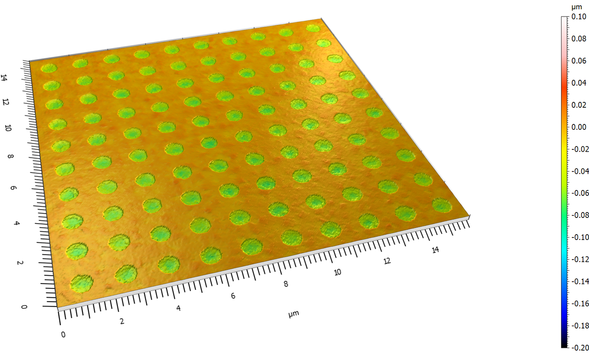
In the present study by Solarius, an inspection of so-called copper pillars was performed. These microscopic copper pillars consist of a cylinder of copper and a small cap of solder and are used in chip manufacturing. They form recesses of a few tens of nanometers embedded in a transparent matrix with diameters and spacings well below one micrometer. In terms of lateral dimension, they are thus at the absolute limit of microscopy.
The image data is acquired in a familiar manner. The height measurement range to be examined is stepped through and a confocal microscope image is acquired for each step. The measuring field is relatively large at over 7,500 μm², so that more than 3,000 of the structures to be examined can be recorded simultaneously. A complex evaluation of the confocal curves is used to assign one or - in layer systems - several height values to each X-Y coordinate. This is where Solarius comes in.

A confocal curve not only contains height and reflection information of an image point, but also extensive information about the imaging errors of the measuring system used. These can be mathematically determined by means of an algorithm and then excluded from the calculation of the surface topography. In this way, objects with even the smallest structures can be detected and measured with high repeatability. The depth vias could be accurately calculated with a repeatability of only 3.7 nm. The determination of the diameters resulted in a repeatability of just 7 nm, which corresponds to less than 1 % of the measured size.
Via this novel evaluation of the determined confocal data, Solarius is able to create realistic 3D images of surfaces even for micro-geometries and the thinnest transparent layers. The 3D measurement method presented here thus enters an unrivaled niche and far surpasses conventional scanning examination methods in terms of measurement speed, area acquisition rate and quality of the optical measurement data.
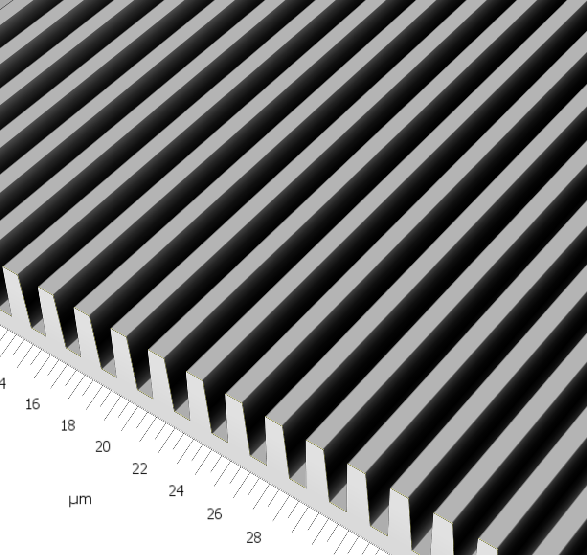
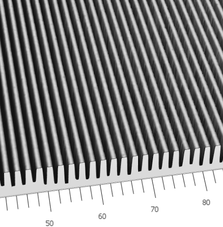
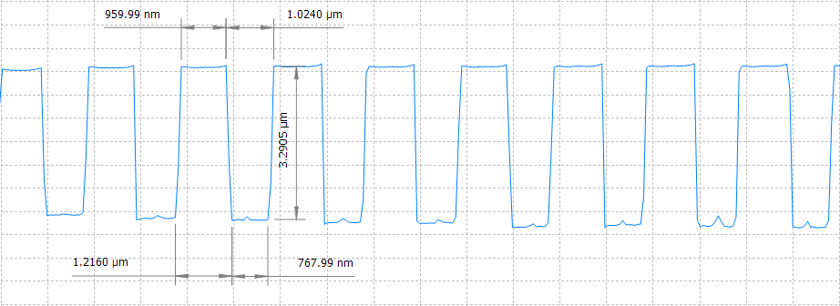
The high quality of the sensor raw data in combination with sophisticated signal processing and intelligent image processing algorithms allows to advance the transitional area of confocal metrology towards the AFM systems domain. In line monitoring of self aligment structures are a good proof to show the Solarius technology lead in confocal 3D imaging. In the image to the right, self aligment structures with a line frequency of 2μm and spacer depth of 3μm are shown. Such live structures can be measured with precision and accuracy values below 1% of the structure size using Solarius Confocal microscopy tools. The process supports line and space structure asessement throughout the diffrent pocess steps. Dimensions can be assessed reliably after lithography in the developed film as well as after etching in silcon.
Supported by the Solarius SIMP front end tools and the Solarius SolarCore software platform, the confocal microscopes deliver fast, robust and reliable process control information. The SIMP tools are available in a compact and space saving version for up to 200 millmeter wafers and in a 200/300 millimeter configuration providing full 300 millimeter SECS/GEM integration and OHT/AGV support on the SEMI E84 protocoll. All tools come with the state of the art SEMI compliant SolarScanSC user interface.