FingerPrint Sensors :
Application & Solutions

Where images are divided into pixels, whether in projection or detection, photo- or light-emitting diodes are used. However, these always require additional electronics, so that the area of each pixel is not determined exclusively by the diode, but by the entire installation space of all necessary parts. The ratio of diode size to total size is called the fill factor and is a decisive criterion for signal quality and the signal-to-noise ratio in cameras. A high fill factor can therefore be achieved either by reducing additional components or by focusing the light on the diode.
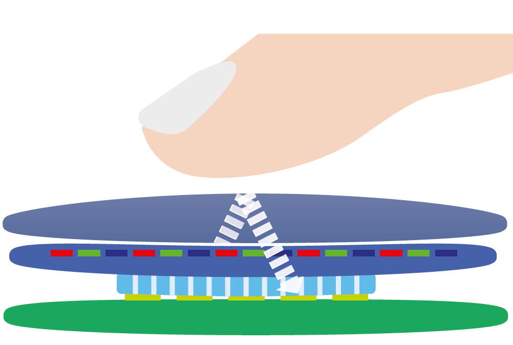
Integrating multiple functions in one device, e.g. integrating finger print sensors in displays, makes it necessary to route light on complex paths from and to different locations within one single device. Such can be done by combining filters and lenses in very dense packages which cannot be recognized by the human eye any more. In this way, microlenses make it possible to create new technologies and applications as well as to build photodiodes and projectors much more effciently.
However, the strength of small lenses lies not only in the replacement of classic optics: wafer-level optics are conceivable in the first place because nowadays optics can be manufactured in the micrometer range. Here, the lenses are manufactured directly by means of industrially tested semiconductor technologies.

In some cases, this approach goes so far that light replaces the electric current in integrated semiconductors. The large-scale use of these miniaturized structures and their strong dependency on the exact adherence to the desired shape requires the monitoring of the process quality. In addition to the material composition, the shape of the lenses is decisive for their optical properties. Due to the long measuring times, tactile measurement methods are only suitable to a limited extent, so that an alternative has to be found.

Optical systems often fail because microlenses are transparent and generate interference and refraction. Solarius confocal microscopes are notable for their ability, unlike many other systems on the market, to image these diffcult surfaces free of aberrations.
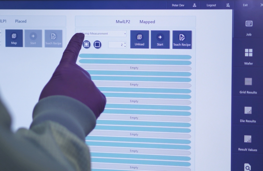
The SEMI wafer processing user interface provides visualization and functionality for wafer handling and metrology workflows. It allows teaching of multi project grid based recipes for wafer and panel shaped substrates, definitiontion of specification limits and the displaying of quality relevant results, taking into account the individual role rights of the current users.
Smart device displays

Almost every smartphone nowadays comes with in-display fingerprint scanners. These are either ultrasonic or optical-capacitive scanners. While smartphones and other wearables using OLED screens prefer to use optical-capacitive scanners, in contrast, ultrasonic scanners are easy and cost- effective to implement.
In display fingerprint scanners make necessary additional functionality within the already complex structure of modern displays. To interpose different functions such as displaying information with the same screen that reads a fingerprint, complex micro lens and filter structures are necessary to be manufactured reliably. Solarius 3D metrology enables the high volume inspection of micro lenses throughout the manufacturing process.
QA relevant parameters
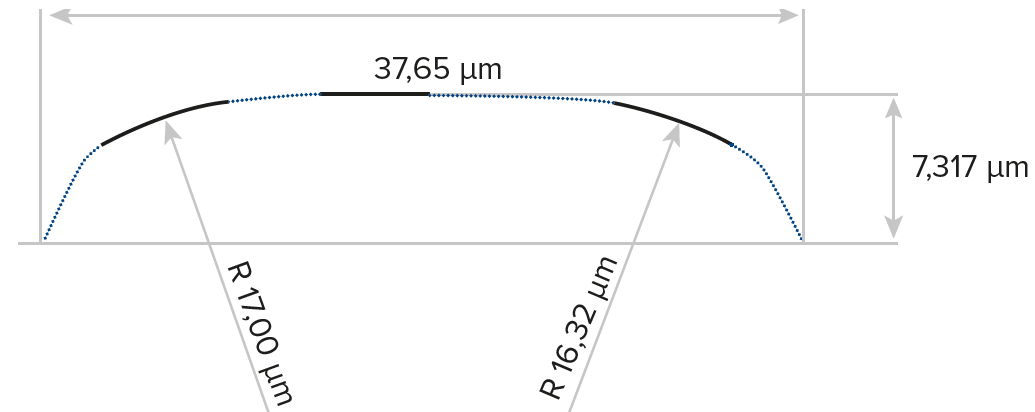
Diameter, edge length, curvature and ellipticity determine the shape of the lens and thus its optical properties. Due to the transmitting behavior of glass, direct measurement of the surface with optical technologies proves diffcult. However, with the robust and highly dynamic confocal sensors and intelligent image processing solutions from Solarius, transparent surfaces can also be easily measured with nanometer accuracy.

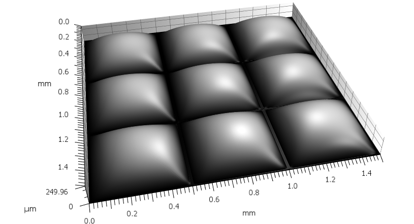
Due to their high number, density and small size, it is uneconomical and usually technically impossible to align microlenses within arrays. As a result, the alignment of lenses must be carried out during production. From the tilting of each individual lens, the optical axis and thus the alignment can be inferred.
Due to the proximity of Solarius measurement systems to the production environment, short-term process adaptations are possible, which minimize production rejects. Micro lenses for sensor devices, in large volumes become manufactured in semiconductor processes on wafers. However, even in production lines that fullfill highest requirements to cleanliness, it can never be completely ruled out that particles may cause contamination. Also, local deformations of microlenses such as indentations or cracks have a signifi cant effect on component function. Solarius measurement technology can detect debris and defects with sizes well below one micrometer and therefore enables a high quality standard to be maintained.