PR Layers & CMP :
Application & Solutions

During the manufacturing of electroplated structures, such as so called copper pillar interconnects or critical dimension strutures, multilayer systems of photoresist are utilized to create form cast structures for subsequent plating processes. For this, metallized wafer surfaces become spin coated with one or more layers of transparent photo resist material before the desired structure is applied to it via lithography, film development and cleaning processes.
After having created the raw cast structure in the resist, conducting materials become deposited inside the openings of the photoresist and grow towards the desired geometry. The structure of the developed photo resist hereby determines the final shape and dimensions of the plated materials.
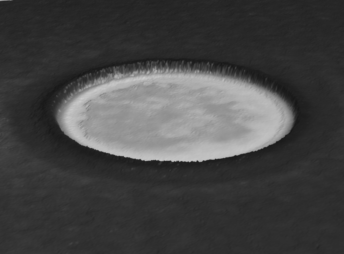
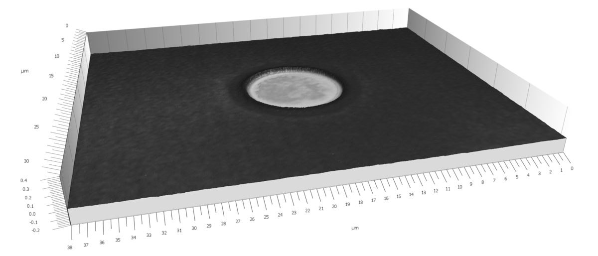
The image shows the top of a copper pillar, still surrounded by the cured photo resist material. The top surface of the copper pillar is not at the same height as the photo resist material. In order to determine the actual height of the copper pillar in respect to the wafer surface, height or thickness measurements of the transparent layer system as well as of the copper pillar surface are important. Also, the co-planarity of the pillar structure throughout the whole wafer is crucial. Determinantion of the layer system as well as the plated material can be performed optically in the nanometer range. Also, such measurements can be performed during CMP, a polishing process which seeks to egalize oxide surfaces and pillar top stand-off. Typically, the abrasion of the oxides and the copper is not homogeneus, due to the different degrees of hardness of invidual materials and for this reason requires frequent QA via process metrology. The profiles below show the copper pillar within the surrounding photo resist layer system.

The copper pillar and its surrounding photo resist layer system was acquired by the usage of the Solarius Polaris confocal microscope technology. The whole data set was acquired within one single data acquistion within a field of view of 87 μm x 87 μm and a sub micron lateral resoultion. The diameter of the copper pillars within the filed of view is about 8 μm.

Typically, confocal systems are known to not have the capability to resolve layer thicknesses below 1μm, reliably. However, due to constant innovation and development in hardware, software and image processing intelligence, Solarius confocal systems are capable to resolve transparent layers down to 100 nanometers, reliably, in certain cases even below.
The Polaris confocal technology is available throughout the complete Solarius product range. It can be obtained as a cost efficient and space saving desk top solution for R&D purposes as well as on the robust and versatile AOP platforms which are suitable to extensive customization. The AOP platforms allow full automatisation of the metrology process and come alnog with SolarScanSC user interface, dsigned accordingly to SEMI and GAMP guidelines. For full fab integration in semiconductor indutsry the Polaris confocal technology is available as well on the SIMP allowing remote control of the metrology via the SECS/GEM standard, including OHT and AGV loading.